

What Is An Adc14 Register
Chapter 14: Analog to Digital Conversion, Data Conquering and Control
Modified to exist compatible with EE319K Lab 8
Jonathan Valvano and Ramesh Yerraballi
Throughout this class we have seen that an embedded system uses its input/output devices to interact with the external world. In this affiliate we will focus on input devices that we use to gather data about the world. More than specifically, we present a technique for the system to mensurate analog inputs using an analog to digital converter (ADC). We will utilise periodic interrupts to sample the ADC at a stock-still rate. We define the rate at which nosotros sample as the sampling charge per unit, and utilize the symbol fs. We will and then combine sensors, the ADC, software, PWM output and motor interfaces to implement intelligent command on our robot machine.
| Learning Objectives:
|
Video xiv.0. Introduction to Digitization |
fourteen.1. Information Acquisition and Control Systems
Video 14.1. Digitization Concepts.
The measurand is a real world indicate of involvement similar sound, distance, temperature, strength, mass, force per unit area, menses, light and acceleration. Figure 14.ane shows the data flow graph for a information acquisition system or control system. x(t) is the fourth dimension-varying indicate nosotros are attempting to mensurate. The command system uses an actuator to drive a measurand in the existent earth to a desired value while the data acquisition organisation has no actuator because it simply measures the measurand in a nonintrusive style. Consider an entire system that collects data, not but the ADC. The following four limitations exist when sampling data.
- Amplitude resolution
- Aamplitude range
- Time quantization
- Time interval
Amplitude resolution is the smallest modify in input signal that can be distinguished. For case, we might specify the resolution as dX. Amplitude range is defined equally the smallest to largest input value that can exist measured. For example, we might specify the range as Xmin to Xmax. Amplitude precision is defined as the number of distinct values from which the measurement is selected. The units of precision are given in alternative or bits. If a system has 12-scrap precision, at that place are 2^12 or 4096 distinct alternatives. For example if we use a slide pot to mensurate distance, the range of that pot might exist 0 to 1.5cm. If there is no electric racket and nosotros use a 12-bit ADC, and so the theoretical resolution is 1.5cm/4095, or about 0.0004 cm. In most systems, the resolution of the measurement is determined by noise and not the number of bits in the ADC. Time quantization is the time difference between one sample and the side by side. Time interval is the smallest to largest time during which we collect samples. If we apply a x-Hz SysTick interrupt to sample the ADC and calculate altitude, the sampling rate, fs, is 10 Hz, and the time quantization is 1/fs=0.1 sec. If we utilize a retentivity buffer with 500 elements, then the fourth dimension interval is 0 to l sec.
: Assume Xmin, Xmax, and dX are all given in the aforementioned units. Give a formula that relates the precision in $.25 as a function of Xmin, Xmax and dX.
: Assume the precision is n in bits, and Xmin, Xmax, and dX are all given in the same units. Give a formula that relates the resolution, dX as a function of Xmin, Xmax and northward.
: Assume you have a 12-bit ADC and store data into an array of type uint16_t. Let fs be the sampling rate in Hz, and T exist the total time interval required to collect samples in sec. Give a formula that relates needed retention in bytes as a function of fs and T.
: Presume you lot have an 8-bit ADC. Allow the sampling rate be 100 Hz. Assume you allocate 20,000 out of the available 32,768 bytes of RAM to store the data. What is the corresponding fourth dimension interval? I.eastward., how many seconds of data can y'all record?
: Assume you lot have a 4-chip DAC used to play audio. Let the sampling rate be 11 kHz. Yous can pack 2 DAC samples into one byte. Assume you allocate 128 kibibytes out of the bachelor 256 kibibytes of ROM to store the data. What is the corresponding fourth dimension interval? I.e., how many seconds of audio can yous play?
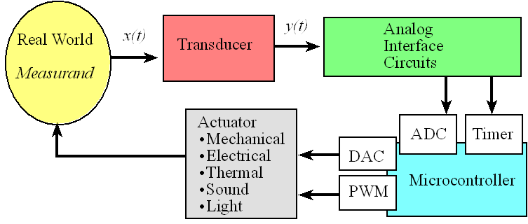
Figure xiv.1. Signal paths a data acquisition system.
The input or measurand is ten. The output is y. A transducer converts x into y. A wide variety of inexpensive sensors can be seen at https://www.sparkfun.com/categories/23 Examples include
· Sound Microphone
· Pressure, mass, forcefulness Strain gauge, force sensitive resistor
· Temperature Thermistor, thermocouple, integrated circuits
· Distance Ultrasound, lasers, infrared light
· Catamenia Doppler ultrasound, flow probe
· Acceleration Accelerometer
· Light Camera
· Biopotentials Silvery-Silvery Chloride electrode
A linear transducer is an input/output part fits a direct line. In other words, the input/output response fits a linear equation:
y = m*x*b
where g and b are constants. Software will have an easy time with a linear transducer. For example, the linear potentiometer, PTA20432015CPB10, has a transfer function as shown in Figure fourteen.2, where the input x is distance in cm, and the output y is resistance in kΩ. Yous tin can employ a simple circuit to catechumen resistance to voltage, the ADC to convert voltage to an integer, and elementary software to catechumen an integer to distance.
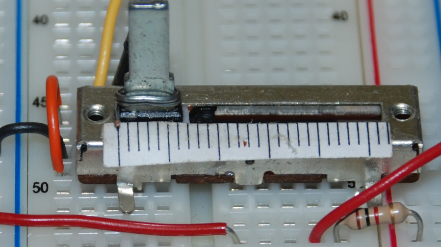
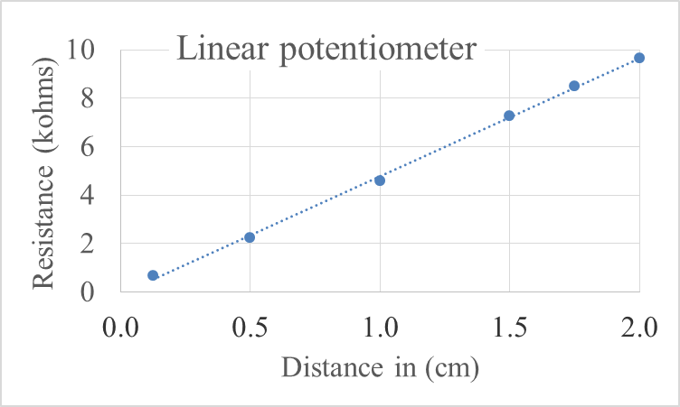
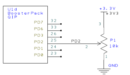
Figure 14.2. The linear potentiometer distance sensor exhibits linear behavior.
: Consider the linear potentiometer in Figure 14.2. Let ten be the distance in cm and allow y be the resistance in kohm. Give an appropriate transfer function showing y as a part of 10.
A nonmonotonic transducer is an input/output part that does non have a mathematical inverse. For case, if ii or more input values yield the same output value, then the transducer is nonmonotonic. Software will have a difficult time correcting a nonmonotonic transducer. For example, the Sharp GP2Y0A21YK IR altitude sensor has a transfer function equally shown in Figure 14.three. If you read a transducer voltage of ii Five, you lot cannot tell if the object is 3 cm abroad or 12 cm abroad. Withal, if we presume the altitude is always greater than 10cm, so this transducer can exist used. Details about transducers and actuators tin be found in Embedded Systems: Real-Time Interfacing to ARM Cortex-M Microcontrollers, 2020, ISBN: 978-1463590154.
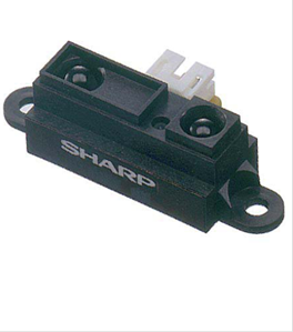
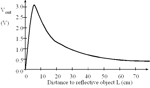
Figure xiv.3. The Precipitous IR altitude sensor exhibits nonmonotonic behavior.
xiv.ii. The Analog to Digital Converter
An analog to digital converter (ADC) converts an analog signal into digital form, shown in Effigy 14.iv. An embedded organisation uses the ADC to collect data nearly the external world (data acquisition system.) The input betoken is unremarkably an analog voltage, and the output is a binary number. The ADC precision is the number of distinguishable ADC inputs (e.g., 4096 alternatives, 12 bits). The ADC range is the maximum and minimum ADC input (e.g., 0 to +iii.3V). The ADC resolution is the smallest distinguishable change in input (east.g., 3.3V/4095, which is almost 0.81 mV). The resolution is the change in input that causes the digital output to modify by 1.
Range(volts) = Precision(alternatives) • Resolution(volts)
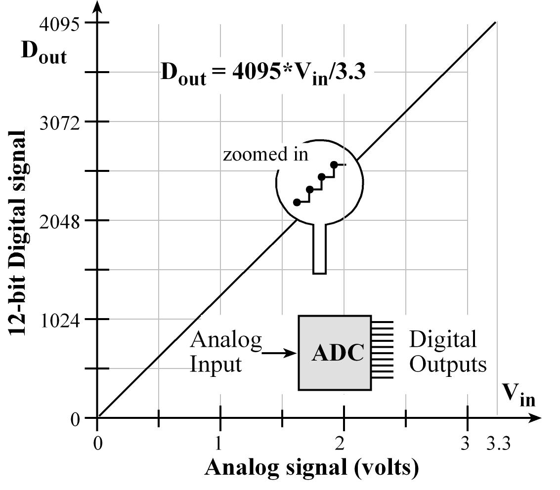
Figure 14.4. A 12-bit ADC converts 0 to 3.3V on its input into a digital number from 0 to 4095.
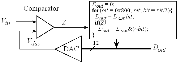
The most pervasive method for ADC conversion is the successive approximation technique, every bit illustrated in Figure xiv.five. A 12-bit successive approximation ADC is clocked 12 times. At each clock some other bit is adamant, starting with the most significant scrap. For each clock, the successive approximation hardware issues a new "guess" on Vdac by setting the bit nether test to a "1". If Vdac is now higher than the unknown input, 5in , then the bit nether test is cleared. If Vdac is less than Vin , and then the bit under test is remains 1. In this clarification, fleck is an unsigned integer that specifies the bit nether exam. For a 12-bit ADC, bit goes 2048, 1024, 512, 256,...,one. Dout is the ADC digital output, and Z is the binary input that is truthful if Vdac is greater than 5in .
| Figure fourteen.5. A 12-chip successive approximation ADC. |
Video 14.2. Successive Approximation |
Interactive Tool xiv.ane
This tool allows you to get through the motions of a ADC sample capture using successive approximation. It is a game to demonstrate successive approximation. There is a hole-and-corner number between 0 to 63 (6-fleck ADC) that the computer has selected. Your job is to learn the hugger-mugger number by making exactly vi guesses. Y'all can guess past entering numbers into the "Enter approximate" field and clicking "Guess". The Tool will tell yous if the number yous estimate is higher or lower than the secret number. When you accept the answer, enter it into the "Final reply" field and click the "Submit answer" button.
The secret number is ???
The cloak-and-dagger number is strictly less than these guesses :
The secret number is greater than or equal to these guesses :
: With successive approximation, what is the strategy when making the first gauge? For example, if you had a 10 bit ADC, what would exist your showtime guess?
Observation: The speed of a successive approximation ADC relates linearly with its precision in $.25.
Usually nosotros don't specify accuracy for only the ADC, only rather we give the accuracy of the entire organisation (including transducer, analog circuit, ADC and software). An ADC is monotonic if it has no missing codes as the analog input slowly rises. This ways if the analog signal is a slowly rising voltage, and so the digital output volition hit all values ane at a time, always going up, never going downward. The figure of merit of an ADC involves three factors:
- precision (number of $.25),
- speed (how fast can nosotros sample), and
- ability (how much energy does it take to operate).
How fast nosotros can sample involves both the ADC conversion time (how long it takes to convert), and the bandwidth (what frequency components can exist recognized by the ADC). The ADC price is a office of the number and quality of internal components. Two 12-chip ADCs are built into the TM4C123 microcontroller, called ADC0 and ADC1. You lot will use ADC0 to collect data and we will use ADC1 and the PD3 pivot to implement a voltmeter and oscilloscope using TExaSdisplay.
xiv.3. Details of the ADC on the TM4C123
Table 14.1 shows the ADC0 register bits required to perform sampling on a single aqueduct. Any bits not specified will read 0. There are two ADCs; yous will employ ADC0 and TExaSdisplay uses ADC1. For more than complex configurations refer to the specific data sail. The value in the ADC0_PC_R specifies the maximum sampling charge per unit, encounter Tabular array 14.2. This is non the actual sampling rate; it is the maximum possible. Setting ADC0_PC_R to vii, allows the TM4C123 to sample upward to ane meg samples per 2nd. The instance code in this department will set ADC0_PC_R to 1, because we volition be sampling much slower than 125 kHz. It will be more accurate and crave less ability to run at 125 kHz maximum way, as compared to one MHz maximum way. In this chapter we will use software trigger mode, and then the bodily sampling rate is determined past the SysTick periodic interrupt charge per unit; the SysTick ISR will take one ADC sample. On the TM4C123, we will need to set $.25 in the AMSEL register to activate the analog interface. Furthermore, we volition clear $.25 DEN register to deactivate the digital interface.
| Accost | 31-17 | xvi | 15-3 | 2 | 1 0 | Proper noun | |||
| 0x400F.E638 | ADC1 ADC0 | SYSCTL_RCGCADC_R | |||||||
| 31-xiv | xiii-12 | 11-ten | 9-8 | 7-6 | 5-4 | 3-ii | 1-0 | ||
| 0x4003.8020 | SS3 | SS2 | SS1 | SS0 | ADC0_SSPRI_R | ||||
| 31-16 | 15-12 | 11-8 | 7-four | 3-0 | |||||
| 0x4003.8014 | EM3 | EM2 | EM1 | EM0 | ADC0_EMUX_R | ||||
| 31-4 | 3 | ii | i | 0 | |||||
| 0x4003.8000 | ASEN3 | ASEN2 | ASEN1 | ASEN0 | ADC0_ACTSS_R | ||||
| 0x4003.8030 | AVE (3 bits) | ADC0_SAC_R | |||||||
| 0x4003.80A0 | MUX0 | ADC0_SSMUX3_R | |||||||
| 0x4003.8FC4 | Speed | ADC0_PC_R | |||||||
| 0x4003.80A4 | TS0 | IE0 | END0 | D0 | ADC0_SSCTL3_R | ||||
| 0x4003.8028 | SS3 | SS2 | SS1 | SS0 | ADC0_PSSI_R | ||||
| 0x4003.8004 | INR3 | INR2 | INR1 | INR0 | ADC0_RIS_R | ||||
| 0x4003.800C | IN3 | IN2 | IN1 | IN0 | ADC0_ISC_R | ||||
| 31-12 | eleven-0 | ||||||||
| 0x4003.80A8 | DATA | ADC0_SSFIFO3 | |||||||
Table fourteen.1. The TM4C ADC registers. Each register is 32 bits wide. Yous will use ADC0 and we will apply ADC1 for the grader and to implement the oscilloscope feature.
| Value | Clarification |
| 0x7 | 1M samples/second |
| 0x5 | 500K samples/second |
| 0x3 | 250K samples/2d |
| 0x1 | 125K samples/2d |
Table 14.2. The maximum sampling rate specified in the ADC0_PC_R register.
Table 14.3 shows which I/O pins on the TM4C123 tin can be used for ADC analog input channels.
| IO | Ain | 0 | 1 | 2 | 3 | 4 | five | six | seven | viii | 9 | xiv |
| PB4 | Ain10 | Port | SSI2Clk | M0PWM2 | T1CCP0 | CAN0Rx | ||||||
| PB5 | Ain11 | Port | SSI2Fss | M0PWM3 | T1CCP1 | CAN0Tx | ||||||
| PD0 | Ain7 | Port | SSI3Clk | SSI1Clk | I2C3SCL | M0PWM6 | M1PWM0 | WT2CCP0 | ||||
| PD1 | Ain6 | Port | SSI3Fss | SSI1Fss | I2C3SDA | M0PWM7 | M1PWM1 | WT2CCP1 | ||||
| PD2 | Ain5 | Port | SSI3Rx | SSI1Rx | M0Fault0 | WT3CCP0 | USB0epen | |||||
| PD3 | Ain4 | Port | SSI3Tx | SSI1Tx | IDX0 | WT3CCP1 | USB0pflt | |||||
| PE0 | Ain3 | Port | U7Rx | |||||||||
| PE1 | Ain2 | Port | U7Tx | |||||||||
| PE2 | Ain1 | Port | ||||||||||
| PE3 | Ain0 | Port | ||||||||||
| PE4 | Ain9 | Port | U5Rx | I2C2SCL | M0PWM4 | M1PWM2 | CAN0Rx | |||||
| PE5 | Ain8 | Port | U5Tx | I2C2SDA | M0PWM5 | M1PWM3 | CAN0Tx |
Table 14.3. Twelve different pins on the TM4C123 can be used to sample analog inputs. The example code volition use ADC0 and PE4/Ch9 to sample analog input. TExaSdisplay uses ADC1 and PD3 to implement the oscilloscope feature.
The ADC has iv sequencers, just you will utilise only sequencer 3 in EE319K Labs eight,9,10 (edX MOOC Labs 14 and 15). We set the ADC0_SSPRI_R register to 0x0123 to make sequencer three the highest priority. Because we are using but 1 sequencer, nosotros just need to make sure each sequencer has a unique priority. We set $.25 15–12 (EM3) in the ADC0_EMUX_R register to specify how the ADC will be triggered. Table 14.4 shows the various means to trigger an ADC conversion. More advanced ADC triggering techniques are presented in the book Embedded Systems: Real-Time Interfacing to ARM® Cortex™-G Microcontrollers. However in this chapter, we use software start (EM3=0x0). The software writes an viii (SS3) to the ADC0_PSSI_R to initiate a conversion on sequencer 3. We can enable and disable the sequencers using the ADC0_ACTSS_R register. There are twelve ADC channels on the TM4C123. Which channel nosotros sample is configured by writing to the ADC0_SSMUX3_R annals. The mapping between channel number and the port pivot is shown in Tabular array xiv.three. For case channel 9 is continued to the pin PE4. The ADC0_SSCTL3_R register specifies the mode of the ADC sample. We set TS0 to measure temperature and clear it to measure the analog voltage on the ADC input pin. We set IE0 and so that the INR3 scrap is set when the ADC conversion is complete, and articulate it when no flags are needed. When using sequencer 3, there is only i sample, so END0 will always be ready, signifying this sample is the end of the sequence. In this class, the sequence volition be but one ADC conversion. We set the D0 fleck to activate differential sampling, such as measuring the analog difference between two ADC pins. In our example, nosotros articulate D0 to sample a single-concluded analog input. Because we set up the IE0 scrap, the INR3 flag in the ADC0_RIS_R annals will be prepare when the ADC conversion is consummate, We articulate the INR3 flake past writing an eight to the eight to the ADC0_ISC_R annals.
| Value | Event |
| 0x0 | Software start |
| 0x1 | Analog Comparator 0 |
| 0x2 | Analog Comparator 1 |
| 0x3 | Analog Comparator 2 |
| 0x4 | External (GPIO PB4) |
| 0x5 | Timer |
| 0x6 | PWM0 |
| 0x7 | PWM1 |
| 0x8 | PWM2 |
| 0x9 | PWM3 |
| 0xF | Always (continuously sample) |
Table fourteen.iv. The ADC EM3, EM2, EM1, and EM0 bits in the ADC_EMUX_R annals.
We perform the following steps to configure the ADC for software start on one aqueduct. Plan fourteen.1 shows a specific details for sampling PE4, which is channel 9. The function ADC0_InSeq3 will sample PE4 using software start and use busy-expect synchronization to expect for completion.
Stride ane. We enable the ADC clock bit 0 in SYSCTL_RCGCADC_R for ADC0.
Stride two. We enable the port clock for the pin that we will exist using for the ADC input.
Footstep 3. We wait for the two clocks to stabilize (some people found extra filibuster prevented difficult faults)
Step 4. Brand that pin an input by writing zero to the DIR register.
Step v. Enable the alternative function on that pin by writing 1 to the AFSEL register.
Pace 6. Disable the digital role on that pin by writing nothing to the DEN annals.
Step 7. Enable the analog function on that pivot by writing one to the AMSEL annals.
Step 8. We ready the ADC0_PC_R register specify the maximum sampling rate of the ADC. In this instance, nosotros will sample slower than 125 kHz, and so the maximum sampling rate is set at 125 kHz. This will require less power and produce a longer sampling fourth dimension, creating a more accurate conversion.
Step nine. We will set the priority of each of the four sequencers. In this case, nosotros are using just one sequencer, and then the priorities are irrelevant, except for the fact that no ii sequencers should have the same priority.
Step 10. Before configuring the sequencer, nosotros need to disable it. To disable sequencer 3, we write a 0 to bit three (ASEN3) in the ADC0_ACTSS_R register. Disabling the sequencer during programming prevents erroneous execution if a trigger event were to occur during the configuration process.
Step xi. We configure the trigger event for the sample sequencer in the ADC0_EMUX_R annals. For this example, we write a 0000 to bits 15–12 (EM3) specifying software start way for sequencer 3.
Step 12. Configure the respective input source in the ADC0_SSMUX3 annals. In this example, we write the channel number to bits 3–0 in the ADC0_SSMUX3_R register. In this example, nosotros sample aqueduct 9, which is PE4.
Step 13. Configure the sample control $.25 in the corresponding nibble in the ADC0_SSCTL3 register. When programming the last nibble, ensure that the Terminate bit is ready. Failure to set the END chip causes unpredictable behavior. Sequencer three has only one sample, then we write a 0110 to the ADC0_SSCTL3_R register. Chip 3 is the TS0 scrap, which we clear because nosotros are not measuring temperature. Bit two is the IE0 chip, which we set because we want to the RIS bit to be set when the sample is complete. Bit i is the END0 scrap, which is prepare considering this is the concluding (and only) sample in the sequence. Bit 0 is the D0 bit, which we clear because we do not wish to apply differential fashion.
Footstep 14. Disable interrupts in ADC by immigration bits in the ADC0_IM_R register. Since we are using sequencer 3, nosotros disable SS3 interrupts past clearing bit three.
Pace 15. We enable the sample sequencer logic by writing a one to the corresponding ASEN3. To enable sequencer 3, we write a 1 to bit 3 (ASEN3) in the ADC0_ACTSS_R annals.
| void ADC0_InitSWTriggerSeq3_Ch9(void){ Plan 14.1. Initialization of the ADC using software start and busy-wait (ADCSWTrigger). |
Video 14.3. ADC Initialization Ritual |
Program 14.two gives a role that performs an ADC conversion. In that location are iv steps required to perform a software-start conversion. The range is 0 to 3.3V. If the analog input is 0, the digital output will be 0, and if the analog input is 3.3V, the digital output volition be 4095.
Digital Sample = (Analog Input (volts) • 4095) / iii.3V(volts)
Step i. The ADC is started using the software trigger. The channel to sample was specified earlier in the initialization.
Step 2. The role waits for the ADC to complete by polling the RIS annals fleck 3.
Pace 3. The 12-scrap digital sample is read out of sequencer three.
Step 4. The RIS bit is cleared by writing to the ISC register.
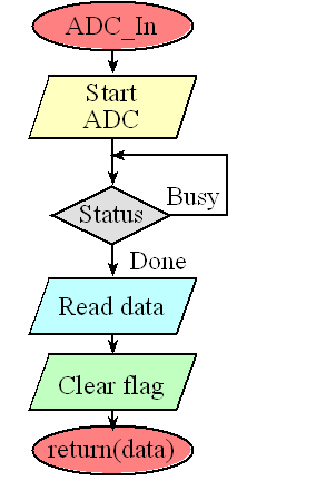
Figure xiv.iii. The four steps of analog to digital conversion: 1) initiate conversion, ii) expect for the ADC to end, 3) read the digital result, and 4) clear the completion flag.
| //------------ADC0_InSeq3------------ // Decorated-wait analog to digital conversion // Input: none // Output: 12-scrap issue of ADC conversion uint32_t ADC0_InSeq3(void){ uint32_t result; ADC0_PSSI_R = 0x0008; // i) initiate SS3 while((ADC0_RIS_R&0x08)==0){}; // two) wait for conversion done result = ADC0_SSFIFO3_R&0xFFF; // three) read result ADC0_ISC_R = 0x0008; // 4) acknowledge completion return result; } Program 14.2. ADC sampling using software start and busy-expect (ADCSWTrigger). |
Video xiv.4. Capturing a Sample |
It is important to sample the ADC at a regular rate. One simple style to deploy periodic sampling is to perform the ADC conversion in a periodic ISR. In the post-obit code, the sampling rate is adamant by the rate of the periodic interrupt. The global variable, Flag is called a semaphore, which is set up when new data is stored into the variable Data. We can connect PF1 to a logic analyzer or oscilloscope to verify the sampling rate.
uint32_t Data; // 0 to 4095
uint32_t Flag; // 1 means new data
void SysTick_Handler(void){
GPIO_PORTF_DATA_R ^= 0x02; // toggle PF1
Data = ADC0_InSeq3(); // Sample ADC
Flag = 1; // Synchronize with other threads
}
At that place is software in the book Embedded Systems: Real-Time Interfacing to ARM® Cortex™-M Microcontrollers showing you how to configure the ADC to sample a single channel at a periodic charge per unit using a timer trigger. The most fourth dimension-accurate sampling method is timer-triggered sampling (EM3=0x5).
: If the input voltage is 1.65V, what value volition the TM4C 12-bit ADC return?
: If the input voltage is 1.0V, what value will the TM4C 12-fleck ADC render?
fourteen.4. Nyquist Theorem
To collect information from the external globe into the computer we must convert information technology from analog into digital form. This conversion procedure is called sampling and considering the output of the conversion is ane digital number at ane bespeak in fourth dimension, at that place must be a finite time in between conversions, Δt. If we use SysTick periodic interrupts, then this Δt is the time between SysTick interrupts. We define the sampling charge per unit every bit
fs = 1/Δt
If this information oscillates at frequency f, then according to the Nyquist Theorem, we must sample that signal at
fs > 2f
Furthermore, the Nyquist Theorem states that if the point is sampled with a frequency of fs , and then the digital samples only incorporate frequency components from 0 to ½ fdue south . Conversely, if the analog betoken does comprise frequency components larger than ½ fsouthward , and so there will be an aliasing fault during the sampling procedure (performed with a frequency of fdue south ). Aliasing is when the digital signal appears to have a different frequency than the original analog signal.
Interactive Tool 14.2:
Discover the Nyquist Theorem. In this blitheness, you command the analog signal by dragging the handle on the left. Click and elevate the handle up and down to create the analog wave (the blue continuous moving ridge). The signal is sampled at a fixed charge per unit (fsouth = 1Hz) (the blood-red wave). The digital samples are connected by direct red lines then you can see the data equally captured by the digital samples in the figurer.
Do 1: If you motion the handle upward and down very slowly y'all will detect the digital representation captures the essence of the analog wave you have created by moving the handle. If you wiggle the handle at a rate slower than ½ fsouthward , the Nyquist Theorem is satisfied and the digital samples faithfully capture the essence of the analog signal.
Do two: However if you wiggle the handle quickly, you lot will observe the digital representation does non capture the analog wave. More specifically, if yous jerk the handle at a rate faster than ½ fdue south the Nyquist Theorem is violated causing the digital samples to be fundamentally different from the analog wave. Endeavor wiggling the handle at a fast only constant charge per unit, and you will observe the digital wave also wiggles but at an incorrect frequency. This wrong frequency is called aliasing.
Figure fourteen.four shows what happens when the Nyquist Theorem is violated. In both cases a signal was sampled at 2000 Hz (every 0.5 ms). In the first figure the 200 Hz betoken is properly sampled, which ways the digital samples accurately draw the analog point. However, in the second figure, the 2200 Hz point is non sampled properly, which means the digital samples exercise not accurately draw the analog point. This mistake is chosen aliasing. Aliasing occurs when the input betoken oscillates faster than the sampling charge per unit and it characterized by the digital samples "looking like" it is oscillating at a dissimilar rate than the original analog signal. For these 2 sets of sampled information, notice the digital data are exactly the same.
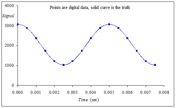
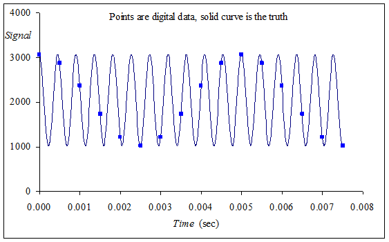
Figure 14.4. Aliasing occurs when the input analog indicate oscillates faster than the rate of the ADC sampling.
Video fourteen.5. Aliasing Demonstration: The Carriage Bike Effect
: Presume you lot wish to represent sounds in digital grade on the computer, either as inputs sampled from an ADC, or as outputs created with a DAC. The approximate range of canine hearing is forty to threescore kHz. What sampling rate preverves all data for canine audio?
: The sounds in Lab x are sampled at xi kHz. What range of frequencies can be in the samples?
: Assume the input is a pure sine wave at one kHz, 1.65+1*sin(2*pi*1k*t), and the ADC is sampled at 2 kHz. Will the data exist properly represented in the digital data?
Valvano Postulate : If fmax is the largest frequency component of the analog signal, and then you must sample more than x times fmax in club for the reconstructed digital samples to wait like the original signal when plotted on a voltage versus fourth dimension graph.
14.v. Central Limit Theorem
The resolution of a measurement system is the smallest change in input that tin be reliably detected. The accuracy of a measurement system is the average departure between measured value and truth. For nigh systems, resolution and accuracy are dominated by noise, rather than the precision of the ADC. To improve signal to noise ratio, we can sample the ADC multiple times and average the samples.
Assume the true signal is μ. More than formally, μ is the expected value of the signal. When we sample the point, noise is added, and then the sampled data does not equal the truth. Let x1, x2, x3,... be sampled data on the same truthful signal. To utilise the Central Limit Theorem (CLT) we will make the post-obit assumptions:
1) the added noise is independent (the added noise of one sample is not related to the added dissonance of another sample);
ii) the added noise has the same probability distribution (whatever physical process that generated the noise in one sample, creates noise in the other samples);
The CLT states that if you have a point with mean μ and standard deviation σ and have sufficiently big random samples (n>30), and summate the boilerplate
X = (sum(x1+x2+...+xn))/n
then the distribution of 10 will exist approximately commonly distributed (Gaussian). More importantly, the expected value of X will approach μ. If the racket has zero hateful (equally likely to be condiment equally subtractive), then X will arroyo the truthful bespeak equally north increases. 1 estimate of dissonance is the standard deviation of multiple samples.
S = sqrt((sum((x1-10)^2+(x2-Ten)^two+...+(xn-Ten)^ii))/n)
In that location is a mode on the ADC to automatically take multiple samples and return the average. The ADC0_SAC_R register tin can be whatever value from 0 to vi. The possible choices are
ADC0_SAC_R = 0; // take 1 sample
ADC0_SAC_R = one; // take ii samples, render boilerplate
ADC0_SAC_R = 2; // take 4 samples, render average
ADC0_SAC_R = 3; // take eight samples, return average
ADC0_SAC_R = 4; // have 16 samples, return average
ADC0_SAC_R = v; // take 32 samples, return average
ADC0_SAC_R = half dozen; // take 64 samples, return average
You will notice the signal to racket ratio will improve dramatically if you use hardware averaging. Withal, the disadvantage of hardware averaging is the time to convert. If taking ane sample takes 8us, then activating 32-point hardware averaging will increase the time to sample to 32*viii=128us. Similarly, information technology will take more than electrical ability to deploy hardware averaging.
Video . Cardinal Limit Theorem
Considering of dissonance, if nosotros set the ADC input to a abiding voltage, and sample it many times, we will get a distribution of digital outputs. Nosotros plot the number of times we got an output equally a office of the output sample. The shape of this response is chosen a probability mass role (pmf) characterizing the noise processes. A pmf plots the number of occurrences versus the ADC sample value. To illustrate the CTL, 1.65V was connected to PE2 and the software in Section fourteen.three was used to measure the ADC m times. The experiment was performed at three values of ADC0_SAC_R: 0 (i point), 2 (4-point average), and 4 (16-point average). Notice the shape becomes Gaussian and the standard deviation reduces. In detail, the information with 1 point (no averaging) has ii or three humps (not normally distributed), just with xvi-point average there is one symmetric hump (normally distributed)
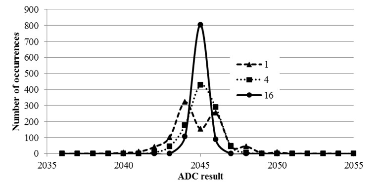
Figure 14.5. Probability mass functions showing hardware averaging improves signal to noise ratio.
: Give an advantage of using hardware averaging.
: Requite ii disadvantages of using hardware averaging.
: The TM4C123 has hardware averaging. What would you practice if y'all want to deploy averaging, just you lot are using a unlike microcontroller that does non support hardware averaging?
14.6. C++ on the TM4C123, EE319H simply
In near aspects, running C++ on the microcontroller is identical to running C++ on other machines. However, be aware of the memory limitations of the TM4C123. To run C++ we volition create a small heap and continue to have a small stack, knowing that all globals, statics, locals, and heap must fit into the 32 kibibytes of RAM on the TM4C123. The following code exists in the startup file for Lab8_C++ project, creating 1024 bytes of stack and 512 bytes of heap.
Stack_Size EQU 0x00000400
Surface area STACK, NOINIT, READWRITE, ALIGN=3
Stack_Mem Infinite Stack_Size
__initial_sp
; Heap Configuration
Heap_Size EQU 0x00000200
AREA HEAP, NOINIT, READWRITE, Align=3
__heap_base
Heap_Mem Space Heap_Size
__heap_limit
Video . Running C++ on the TM4C123.
Video . Running a vector.cpp C++ example from EE312H on the TM4C123.
EE319K Lab eight videos
Educational Objectives of Lab 8
• Sampling
— ADC conversion
— Interrupt-driven periodic sampling
— Calibration and accurateness
— Nyquist Theorem
— Primal Limit Theorem
• Thread synchronization
— Mail box
• Fixed-indicate numbers
— Value = Integer*Constant
• Modular development
• Object oriented design in C++ (EE319H)
Lab8_Introduction
In this video we review the software starter project and overview the blueprint steps for implementing Lab viii. The total scale range of the measurement is determined by the physical size of the potentiometer (some move 0 to 1.5cm, and others movement 0 to 2.0cm).
Lab8_SlidePot
Nosotros show how to adhere slide pot to protoboard. This slide potentiometer has a range of 0 to two cm.
Lab8_Calibration
In this video we demonstrate the steps to calibrate the device. Nosotros actuate hardware averaging to improve betoken to noise ratio
Lab8_Accuracy
In this video nosotros demonstrate the steps to determine accuracy of the device. We will also show yous how to judge resolution. We activate hardware averaging to improve signal to noise ratio.
Collect ii to v measurements with your distance measurement system. In the left column place the true distances as determined by your optics looking at the cursor and the ruler. In the right column place the measured distances as determined by your system. When yous have entered at least 2 sets of data, click the "Calculate" button.
True values | Measured values | Errors
The number of data sets is
The maximum error is
The boilerplate error is
Lab8_Demo
Demonstration of Lab 8 final solution
fourteen.7. Robot Car Controller, EE319K/EE319H students can skip department 14.7
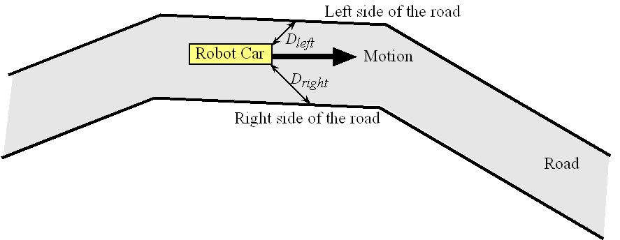
The goal is to drive a robot car apart down a road. Autonomous driving is a difficult problem, and we accept greatly simplified it and volition use this simple problem to illustrate the components of a control organization. Every control system has existent-earth parameters that it wishes to control. These parameters are chosen state variables. In our system we wish to drive down the centre of the road, and then our country variables will be the altitude to the left side of the road and the distance to the right side of the route as illustrated in Figure fourteen.7. When we are in the centre of the road these 2 distances will be equal. So, allow'south define Error as:
Fault = Dleft – Dright
If Error is aught nosotros are in the heart of the road, so the controller volition attempt to drive the Mistake parameter to zero.
| Figure fourteen.7. Physical layout of the autonomous robot as is drives down the road. |
Video 14.6a. IR Sensor for Robot Machine |
Nosotros will need sensors and a data acquisition system to measure Dleft and Dright . In lodge to simplify the problem we volition identify pieces of wood to create walls forth both sides of the road, and make the road the same width at all places along the track. The Sharp GP2Y0A21YK0F infrared object detector can measure distance (http://www.sharpsma.com) from the robot to the wood. This sensor creates a continuous analog voltage between 0 and +3V that depends inversely on distance to object, run across Figure 14.6. We will avoid the 0 to 10 cm range where the sensor has the nonmonotonic beliefs. We will utilize two ADC channels (PE4 and PE5) to convert the ii analog voltages to digital numbers. Let Left and Right be the ADC digital samples measured from the two sensors. We tin assume distance is linearly related to 1/voltage, nosotros can implement software functions to calculate distance in mm as a role of the ADC sample (0 to 4095). The 241814 constant was found empirically, which means we collected data comparison actual distance to measured ADC values.
Dleft = 241814/ Left
Dright = 241814/ Correct
Figure 14.8 shows the accurateness of this data conquering system, where the estimated altitude, using the above equation, is plotted versus the true distance.
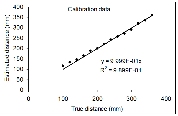
Figure xiv.8. Measurement accuracy of the Sharp GP2Y0A21YK0F distance sensor used to measure distance to wall.
Side by side nosotros need to extend the robot congenital in Instance 12.ii. First nosotros build 2 motor drivers and connect 1 to each bike, as shown in Figure 14.nine. There will be two PWM outputs: PA6 controls the right motor attached to the correct wheel, and PA5 controls the left motor attached to the left wheel. The motors are classified as actuators because they exert force on the world. Like to Example 12.2 we volition write software to create two PWM outputs so we can independently adapt power to each motor. If the friction is abiding, the resistance of the motor, R, volition be fixed and the power is
Ability = (eight.42/R)*H/(H+L)
When creating PWM, the period (H+L) is fixed and the duty bike is varied by irresolute H. Then we meet the robot controller changes H, it has a linear effect on delivered ability to the motor.
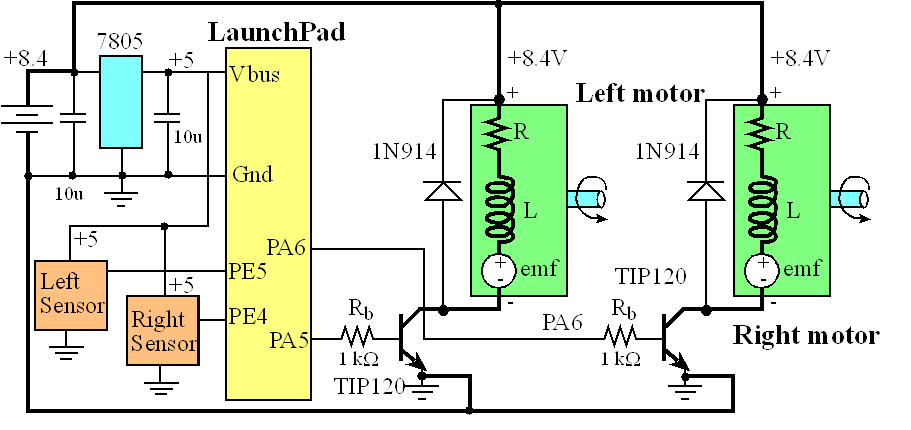
Effigy 14.ix. Circuit diagram of the robot car. One motor is wire reversed from the other, because to move forwards 1 motor must spin clockwise while the other spins counterclockwise.
The currents can range from 500mA to 1 A, and then TIP120 Darlington transistors are used, because they can sink up to three A see data sheet. Discover the dark black lines in Figure 14.ix; these lines signify the paths of these large currents. Detect also the currents do not pass into or out of the LaunchPad. Effigy fourteen.ten shows the robot motorcar. The ii IR sensors are positioned in the front at nigh 45 degrees.
| Figure 14.ten. Photograph of the robot car. |
Video fourteen.7. Autonomous Robot Demonstration |
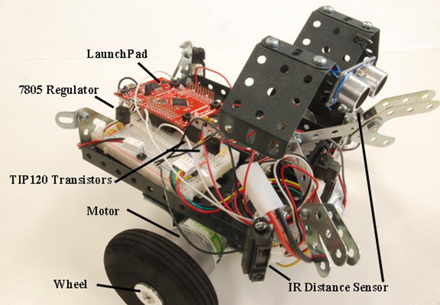
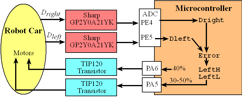
Figure 14.eleven illustrates the feedback loop of the control system. The state variables are Dleft and Dcorrect . The 2 sensors create voltages that depend on these two country variables. The ADC samples these two voltages, and software calculates the estimates Dleft and Dright . Error is the difference betwixt Dleft and Dright . The correct motor is powered with a constant duty cycle of 40%, while the duty cycle of the left motor is adapted in an try to drive down the eye of the road. Nosotros volition constrain the duty bike of the left motor to between xxx% and l%, so it doesn't over compensate and spin in circles. If the robot is closer to the left wall ( Dleft < Dright ) the error volition exist negative and more ability will be practical to the left motor, turning information technology right. Conversely, if the robot is closer to the right wall ( Dleft > Dright ) the error will be positive and less ability will exist applied to the left motor, turning it left. In one case the robot is in the middle of the road, error volition exist naught, and power will not be inverse. This control algorithm can exist written every bit a ready of simple equations. The number "200" is the controller proceeds and is found by trial and error one time the robot is placed on the road. If it is tiresome to react, then we increase gain. If information technology reacts likewise quickly, we decrease the proceeds.
Error = Dleft - Dright
LeftH = LeftH – 200*Error;
if(LeftH < xxx*800) LeftH=30*800; // 30% min
if(LeftH > 50*800) LeftH=l*800; // 50% max
LeftL = 80000 - LeftH; // abiding period
Observation: In the field of control systems, a popular approach is called PID command, which stands for proportional integral derivative. The above simple algorithm really implements the integral term of a PID controller. Furthermore, the ii if statements in the control software implement a characteristic called anti-reset windup.
These controller equations are executed in the SysTick ISR so the controller runs at a periodic rate.
| Figure fourteen.11. Cake diagram of the closed loop used in the robot machine. |
Video fourteen.6b. The Robot Control Organization |
Details nigh microcontroller-based command systems can exist found in Affiliate 10 of Embedded Systems: Real-Time Operating Systems for ARM® Cortex-M Microcontrollers, 2014, ISBN: 978-1466468863.
Pecker of Materials
1) Ii DC geared motors, HN-GH12-1640Y,GH35GMB-R, Jameco Function no. 164786
- 0.23in or 6 mm shaft (get hubs to lucifer)
two) Metal or wood for base of operations,
3) Hardware for mounting
- 2 motor mounts 1-ane/4 in. PVC Conduit Clamps Model # E977GC-CTN Shop SKU # 178931 www.homedepot.com
- some way to attach the LaunchPad (I used an Erector set, but you could employ safety bands)
4) Two wheels and two hubs to friction match the diameter of the motor shaft
- Shepherd 1-1/4 in. Pulley Prophylactic Bike Model # 9487 www.homedepot.com
- 2 6mm hubs Dave'south Hubs - 6mm Hub Set of 2 Part# 0-DWH6MM world wide web.robotmarketplace.com
- 2 3-Inch Bore Treaded Lite Flite Wheels 2pk Office# 0-DAV5730 www.robotmarketplace.com
five) Two GP2Y0A21YK IR range sensors
- Sparkfun, www.sparkfun.com SEN-00242 or http://www.parallax.com/product/28995
half dozen) Battery
- eight.4V NiMH or eleven.1V LiIon. I bought the 8.4V NiMH batteries yous run into in the video as surplus a long time agone. I teach a existent-time Bone class where students write an OS then deploy it on a robot. I have a large pile of these 8.4V batteries, so I used a couple for the two robots in this class. NiMH are easier to charge, simply I advise Li-Ion because they store more energy/weight. For my medical instruments, I use a lot of Tenergy 31003 (7.4V) and Tenergy 31012 (11.1V) (internet search for the all-time price). You will need a Li-Ion charger. I have used both of these Tenergy TLP-4000 and Tenergy TB6B chargers.
7) Electronic components
- two TIP120 Darlington NPN transistors
-2 1N914 diodes
-two 10uF tantalum caps
- 7805 regular
-ii 10k resistors
Websites to buy robot parts
Robot parts
Pololu Robots and Electronics
Jameco'due south Robot Store
Robot Market place
Sparkfun
Parallax
Tower Hobbies
Surplus parts
BG Micro
All Electronics
Full-service parts
Newark (Usa) or element14 (worldwide)
Digi-Key
Mouser
Jameco
Part search engine
Octopart
Reprinted with approving from Embedded Systems: Introduction to ARM Cortex-M Microcontrollers, 2014, ISBN: 978-1477508992, http://users.ece.utexas.edu/~valvano/arm/outline1.htm
from Embedded Systems: Real-Fourth dimension Interfacing to ARM Cortex-Thousand Microcontrollers, 2014, ISBN: 978-1463590154, http://users.ece.utexas.edu/~valvano/arm/outline.htm
and from Embedded Systems: Real-Fourth dimension Operating Systems for the ARM Cortex-1000 Microcontrollers , 2014, ISBN: 978-1466468863, http://users.ece.utexas.edu/~valvano/arm/outline3.htm

Embedded Systems - Shape the World by Jonathan Valvano and Ramesh Yerraballi is licensed nether a Creative Commons Attribution-NonCommercial-NoDerivatives 4.0 International License.
Based on a piece of work at http://users.ece.utexas.edu/~valvano/arm/outline1.htm.

What Is An Adc14 Register,
Source: https://users.ece.utexas.edu/~valvano/Volume1/E-Book/C14_ADCdataAcquisition.htm
Posted by: whitehatian.blogspot.com
0 Response to "What Is An Adc14 Register"
Post a Comment